- 您现在的位置:买卖IC网 > Sheet目录2006 > LTC2306CDD#PBF (Linear Technology)IC ADC 12BIT 2CH 500KSPS 10-DFN
LTC2302/LTC2306
13
23026fa
APPLICATIONS INFORMATION
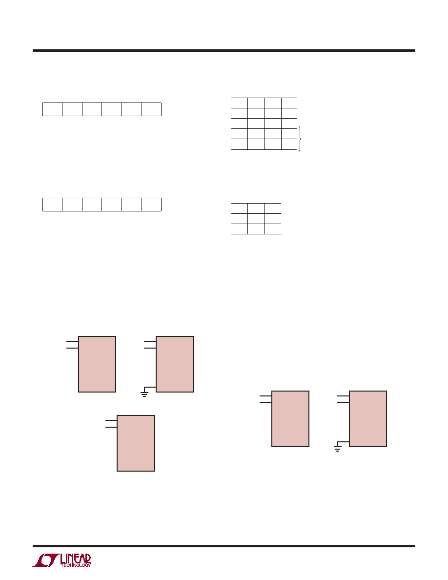
Figure 1a. Example MUX Congurations
Figure 1b. Changing the MUX Assignment “On the Fly”
and Control section). The input data word for the LTC2306
is dened as follows:
S/D O/S
X
UNI
X
S/D = SINGLE-ENDED/DIFFERENTIAL BIT
O/S = ODD/SIGN BIT
UNI = UNIPOLAR/BIPOLAR BIT
X = DON’T CARE
For the LTC2302, the input data word is dened as:
X
O/S
X
UNI
X
Analog Input Multiplexer
The analog input MUX is programmed by the S/D and O/S
bits of the DIN word for the LTC2306 and the O/S bit of the
DIN word for the LTC2302. Table 1 and Table 2 list MUX
congurations for all combinations of the conguration
bits. Figure 1a shows several possible MUX congurations
and Figure 1b shows how the MUX can be recongured
from one conversion to the next.
Driving the Analog Inputs
The analog inputs of the LTC2302/LTC2306 are easy to
drive. Each of the analog inputs of the LTC2306 (CH0
and CH1) can be used as a single-ended input relative
to GND or as a differential pair. The analog inputs of the
LTC2302 (IN+, IN–) are always congured as a differential
pair. Regardless of the MUX conguration, the “+” and “–”
inputs are sampled at the same instant. Any unwanted
signal that is common to both inputs will be reduced by
the common mode rejection of the sample-and-hold cir-
cuit. The inputs draw only one small current spike while
CH0
CH1
(–) GND
2 Single-Ended
+
1 Differential
+ (–)
+
LTC2306
23026 F01a
– (+){
CH0
CH1
1 Differential
+ (–)
LTC2302
– (+){
IN+
IN–
CH0
CH1
(–) GND
LTC2306
2nd Conversion
+
1st Conversion
+
23026 F01b
–{
CH0
CH1
LTC2306
S/D
0
1
O/S
0
1
0
1
CH0
+
–
+
CH1
–
+
WITH RESPECT
TO GND
NOTE: UNIPOLAR MODE SHOULD BE USED
FOR SINGLE-ENDED OPERATION, SINCE INPUT
SIGNALS ARE ALWAYS REFERENCED TO GND
Table 1. Channel Conguration
for the LTC2306
O/S
0
1
IN+
+
–
IN–
–
+
Table 2. Channel Conguration
for the LTC2302
发布紧急采购,3分钟左右您将得到回复。
相关PDF资料
LTC2351HUH-12#TRPBF
IC ADC 12BIT 1.5MSPS 32-QFN
LTC2351HUH-14#TRPBF
IC ADC 14BIT 1.5MSPS 32-QFN
LTC2355IMSE-14#TRPBF
IC ADC 14BIT 3.5MSPS 10-MSOP
LTC2356IMSE-14#TRPBF
IC ADC 14BIT 3.5MSPS 10-MSOP
LTC2366HTS8#TRPBF
IC ADC 12BIT 3MSPS TSOT23-8
LTC2379HMS-18#PBF
IC ADC 18BIT SPI/SRL 16MSOP
LTC2380HMS-16#TRPBF
IC ADC 16BIT 2MSPS 16-MSOP
LTC2382HMS-16#PBF
IC ADC 16BIT 1CH 500KSPS 16-MSOP
相关代理商/技术参数
LTC2306CDD#TRPBF
功能描述:IC ADC 12-BIT 2CH 500KSPS 10DFN RoHS:是 类别:集成电路 (IC) >> 数据采集 - 模数转换器 系列:- 标准包装:2,500 系列:- 位数:16 采样率(每秒):15 数据接口:MICROWIRE?,串行,SPI? 转换器数目:1 功率耗散(最大):480µW 电压电源:单电源 工作温度:-40°C ~ 85°C 安装类型:表面贴装 封装/外壳:38-WFQFN 裸露焊盘 供应商设备封装:38-QFN(5x7) 包装:带卷 (TR) 输入数目和类型:16 个单端,双极;8 个差分,双极 配用:DC1011A-C-ND - BOARD DELTA SIGMA ADC LTC2494
LTC2306IDD#PBF
功能描述:IC ADC 12BIT 2CH 500KSPS 10-DFN RoHS:是 类别:集成电路 (IC) >> 数据采集 - 模数转换器 系列:- 标准包装:2,500 系列:- 位数:16 采样率(每秒):15 数据接口:MICROWIRE?,串行,SPI? 转换器数目:1 功率耗散(最大):480µW 电压电源:单电源 工作温度:-40°C ~ 85°C 安装类型:表面贴装 封装/外壳:38-WFQFN 裸露焊盘 供应商设备封装:38-QFN(5x7) 包装:带卷 (TR) 输入数目和类型:16 个单端,双极;8 个差分,双极 配用:DC1011A-C-ND - BOARD DELTA SIGMA ADC LTC2494
LTC2306IDD#TRPBF
功能描述:IC ADC 12-BIT 2CH 500KSPS 10DFN RoHS:是 类别:集成电路 (IC) >> 数据采集 - 模数转换器 系列:- 标准包装:2,500 系列:- 位数:16 采样率(每秒):15 数据接口:MICROWIRE?,串行,SPI? 转换器数目:1 功率耗散(最大):480µW 电压电源:单电源 工作温度:-40°C ~ 85°C 安装类型:表面贴装 封装/外壳:38-WFQFN 裸露焊盘 供应商设备封装:38-QFN(5x7) 包装:带卷 (TR) 输入数目和类型:16 个单端,双极;8 个差分,双极 配用:DC1011A-C-ND - BOARD DELTA SIGMA ADC LTC2494
LTC2308CUF#PBF
功能描述:IC ADC 12BIT 8CH 500KSPS 24-QFN RoHS:是 类别:集成电路 (IC) >> 数据采集 - 模数转换器 系列:- 标准包装:1,000 系列:- 位数:16 采样率(每秒):45k 数据接口:串行 转换器数目:2 功率耗散(最大):315mW 电压电源:模拟和数字 工作温度:0°C ~ 70°C 安装类型:表面贴装 封装/外壳:28-SOIC(0.295",7.50mm 宽) 供应商设备封装:28-SOIC W 包装:带卷 (TR) 输入数目和类型:2 个单端,单极
LTC2308CUF#PBF
制造商:Linear Technology 功能描述:A/D Converter (A-D) IC
LTC2308CUF#TRPBF
功能描述:IC ADC 12BIT 500KSPS 24-QFN RoHS:是 类别:集成电路 (IC) >> 数据采集 - 模数转换器 系列:- 标准包装:1,000 系列:- 位数:16 采样率(每秒):45k 数据接口:串行 转换器数目:2 功率耗散(最大):315mW 电压电源:模拟和数字 工作温度:0°C ~ 70°C 安装类型:表面贴装 封装/外壳:28-SOIC(0.295",7.50mm 宽) 供应商设备封装:28-SOIC W 包装:带卷 (TR) 输入数目和类型:2 个单端,单极
LTC2308CUFPBF
制造商:Linear Technology 功能描述:ADC 12-Bit 8-Ch 500Ksps Low Noise QFN24
LTC2308IUF#PBF
功能描述:IC ADC 12BIT 8CH 500KSPS 24-QFN RoHS:是 类别:集成电路 (IC) >> 数据采集 - 模数转换器 系列:- 标准包装:1 系列:microPOWER™ 位数:8 采样率(每秒):1M 数据接口:串行,SPI? 转换器数目:1 功率耗散(最大):- 电压电源:模拟和数字 工作温度:-40°C ~ 125°C 安装类型:表面贴装 封装/外壳:24-VFQFN 裸露焊盘 供应商设备封装:24-VQFN 裸露焊盘(4x4) 包装:Digi-Reel® 输入数目和类型:8 个单端,单极 产品目录页面:892 (CN2011-ZH PDF) 其它名称:296-25851-6